Helmut-Fischer FISCHERSCOPE® X-RAY XDV-µ® WAFER

Helmut-Fischer FISCHERSCOPE® X-RAY XDV-µ® WAFER

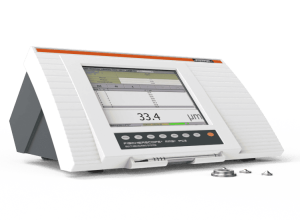
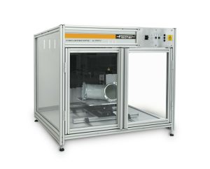
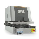
Specialized XRF solution for automated measurements of thin films and multilayer systems on wafers with diameters from 6 – 12 inches.

Meets all requirements for accurate wafer control.

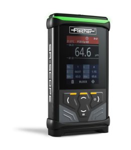
The FISCHERSCOPE® X-RAY XDV®-µ WAFER is optimally tailored to the needs of the semiconductor industry due to its programmable measuring table with vacuum wafer chuck and microfocus tube Ultra. Polycapillary optics built into the XRF device concentrate X-ray radiation on smallest measuring spots of 10 or 20 µm for short measuring times at high intensity. This allows you to analyze individual microstructures much more precisely than with conventional devices – and completely automated.

  • Fully integrated solution.

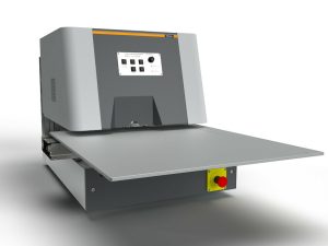
XDV®-μ SEMI combined with wafer handler of your choice

  • Fully automatable.

Let your device work for you with just one click

  • Programmable.

Automated measurements on predefined structures thanks to advanced pattern recognition technology

  • Most advanced polycapillary optics on the market.

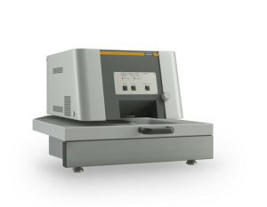
Our in-house manufactured polycapillary optics deliver outstanding measurement results with short measuring times

  • Meeting all challenges.

Reliable and fast results for ambitious measuring tasks

  • DPP+ digital pulse processor.

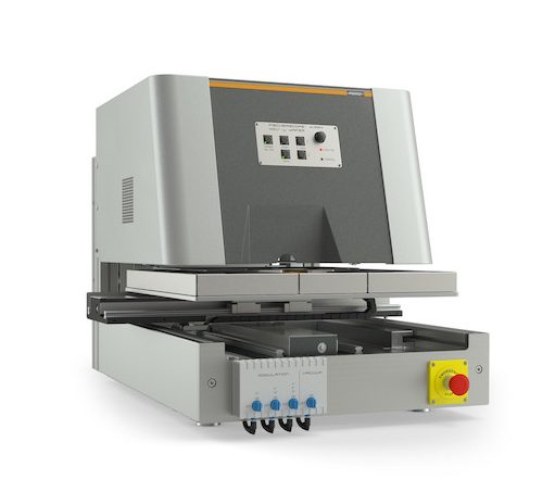
Shorter measuring times or improvement of standard deviation*
*compared to the DPP

  • Microfocus tube Ultra with tungsten anode for even higher performance on smallest spots with µ-XRF; Molybdenum anode optional
  • DPP+ for highest precision even with short measuring times
  • 4-fold changeable filter
  • In-house manufactured polycapillary optics allow especially small measuring spots with high intensity
  • Measuring spot approx.: Ø 10 or 17 µm (FWHM)
  • Up to 5 mm possible height of samples
  • Silicon drift detector with 20 or 50 mm² for highest precision on thin layers
  • Vacuum table with holders for all standard wafer formats from 150 – 300 mm
  • Extensive options for automation with WinFTM®
  • Measuring of smallest structures on wafers up to 12 inch diameter
  • Analysis of very thin coatings, such as gold/palladium layers down to < 10 nm
  • Automated measuring such as in quality control
  • Determination of complex multilayer systems