Helmut-Fischer FISCHERSCOPE® X-RAY XDV®-µ PCB

Helmut-Fischer FISCHERSCOPE® X-RAY XDV®-µ PCB

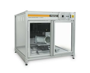
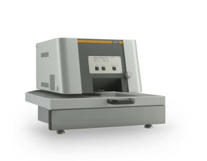
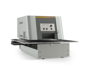
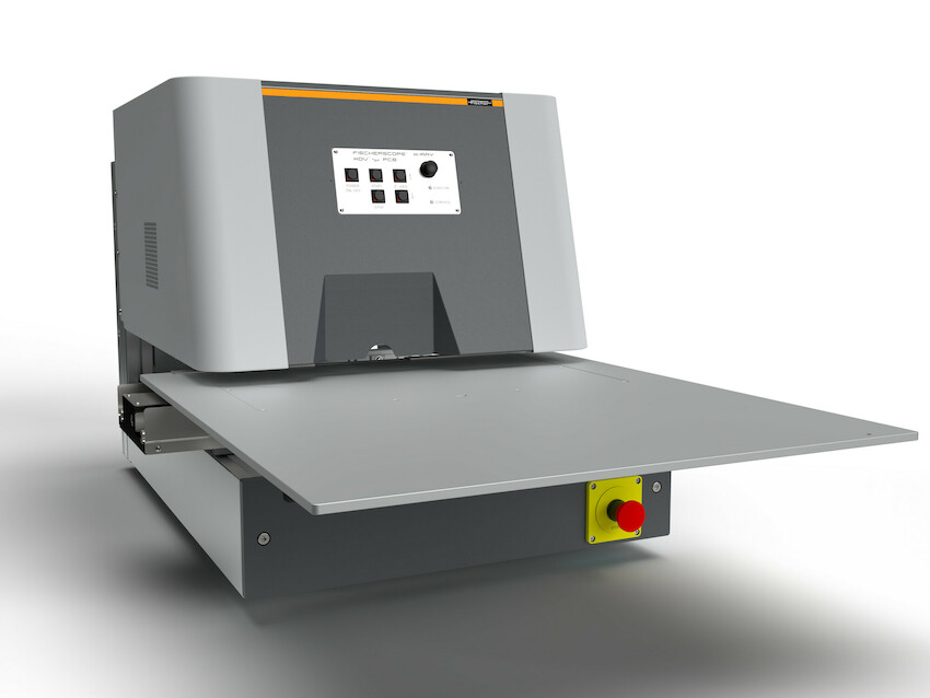
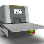
Reliable and fully automatic! Our XDV®-µ PCB devices are the specialized solution for measuring the smallest structures as well as very thin coatings on PCBs.

Automated XRF quality control of PCBs.

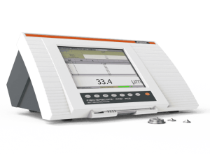
The FISCHERSCOPE® X-RAY XDV®-µ PCB is specially engineered for reliable quality control of PCBs with X-ray fluorescence. Thanks to a powerful silicon drift detector, microfocus tube Ultra and polycapillary optics, the XRF instrument measures with an extremely small measuring spot at very high intensity. This allows you to reliably determine even the thinnest layers. The devices also meet IPC requirements 4552 and 4556 for ENIG and ENEPIG as well as 4553A (Silver) and 4554 (Tin).

  • Meeting all challenges.

Reliable and fast results for ambitious measuring tasks

  • Fully automatable.

Let your instrument work for you

  • PCB experts.

Specialized measuring solutions for printed circuit boards, fulfill IPC standards

  • Most advanced polycapillary optics on the market.

Our in-house manufactured polycapillary optics deliver outstanding measurement results in short measuring times

  • Programmable.

Automated measurements on predefined structures thanks to advanced pattern recognition technology

  • Commissioning.

Extremely fast and simple

  • DPP+ digital pulse processor.

Shorter measuring times or improvement of standard deviation*
*compared to the DPP

  • Microfocus tube Ultra with tungsten anode for even higher performance on smallest spots; Molybdenum anode optional
  • 4-fold changeable filters
  • Up to 10 mm possible height of samples
  • Polycapillary optics allow particularly small measuring spots with short measuring times at high intensity
  • Measuring spot approx.: Ø 10 or 17 µm (FWHM)
  • High-precision, programmable measuring table for PCBs up to 610 x 610 mm, optionally with vacuum fixture
  • Silicon drift detector with 20 or 50 mm² for highest precision on thin films
  • DPP+ for highest precision even with short measuring times
  • Measuring on smallest flat components and structures on PCBs up to 610 x 610 mm (24 x 24 in)
  • Analysis of very thin coatings, such as gold/palladium layers of ≤ 3 nm or 10 nm
  • Automated measuring such as in quality control
  • With the 10 μm option: Measuring with smallest measuring spot in combination with a large silicon drift detector
  • With the vacuum table option: Measuring on flexible PCBs
  • Full compliance with IPC standards 4552 and 4556 (ENIG, ENEPIG), 4553A (Silver) and 4554 (Tin)